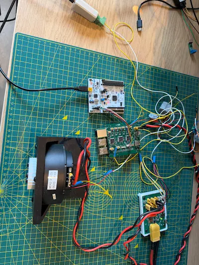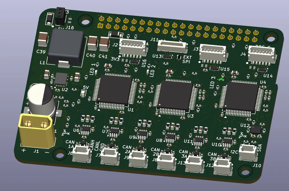

The communication (aka comms) board was needed as a means to interface between the control board (the Raspberry Pi), and the hardware such as motors, while also providing a means of powering the Raspberry Pi from the battery (via the distribution board).
The remainder of the comms board functionality unfolded from there.
An IMU in the torso is also needed so seemed worthwhile including on the board, as opposed to an external connection.
Some LEDs to help development, one per MCU.
A connector for an external SPI/GPIO interface, probably for a wifi module like the NRF24L01 modules I have. How this use differs to the onboard Raspberry Pi wifi needs to be better looked into.
An I2C external connector, for other potential uses.
External power for 3.3V and 5V, again for other potential uses.
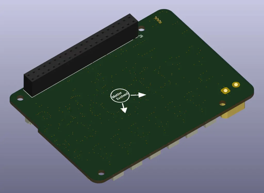
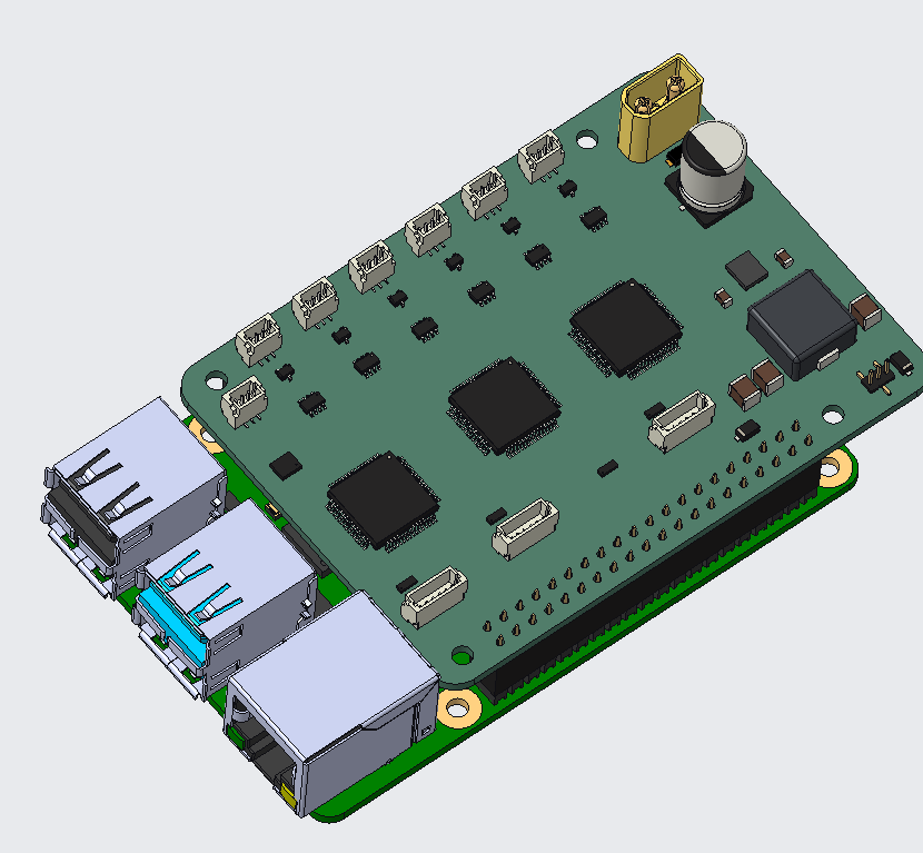
The entire board is intended to mount direct on the Raspberry Pi 4 without expanding the footprint (it does in one direction).
While creating the layout, I though I also may as well connect the three MCUs with a shared SPI bus, and MCU A to the Pi through UART. I’m not sure what I’ll use these for, if I even use them, but I thought I may make as well make the most of having the connections than wanting them later. I could maybe used them for some form of comms board configuration.
Initially, I intended to have more features/components on the board. These were removed largely due to space.
These were things such as:
- Reset buttons for each MCU. Instead need to do it through software or shorting of NRST pin.
- 5V to 3.3V LDO. The Raspberry Pi does this onboard which it makes available through the GPIO so plan to leverage this.
The System
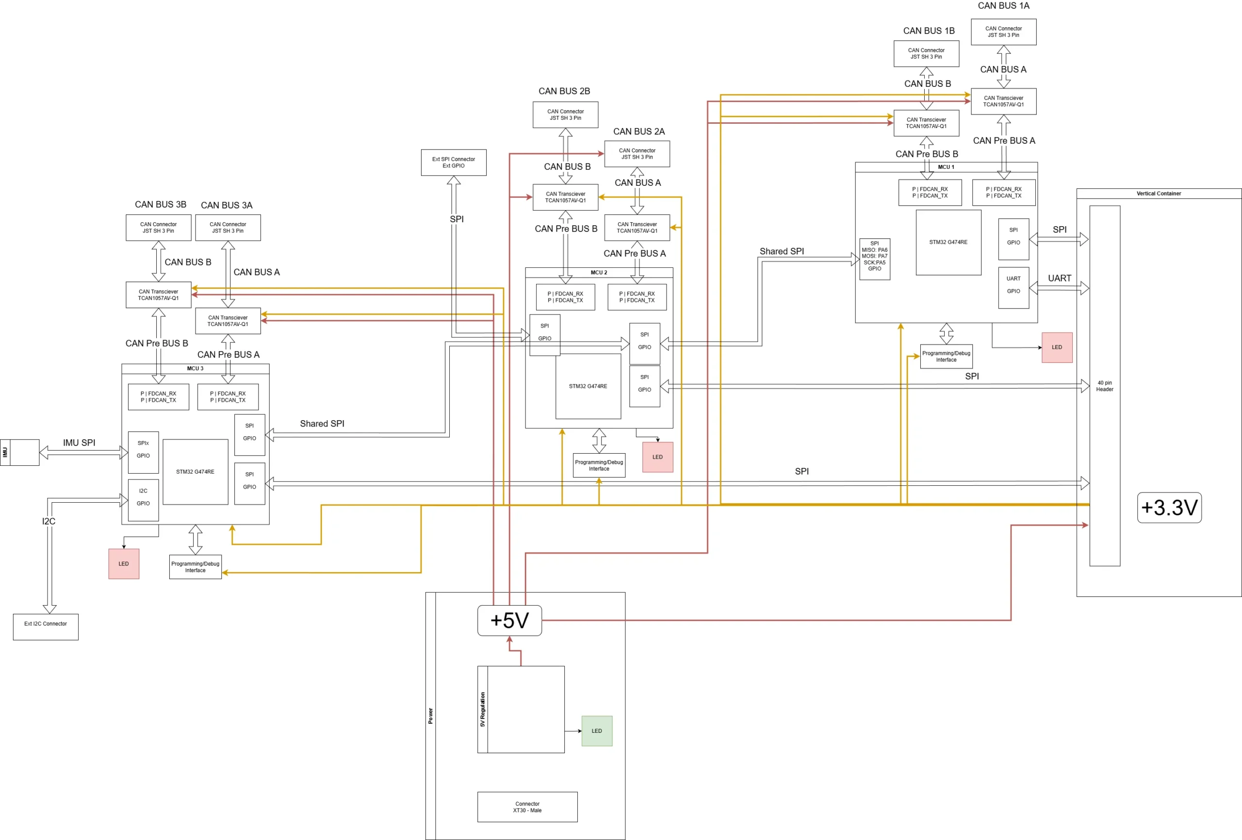
The main functional blocks to develop were
- Power regulation from battery input (via power distribution board) to 5V, through a buck converter
- CAN interfaces
- IMU and its interface
- MCUs
- External connectors
- Raspberry Pi interface
Power Regulation
I wanted to try and allow for as wide a range of input voltage as possible to allow for different size batteries.
As this project is intended to use a 6S LiPo battery I leant towards that voltage. The output voltage needs to 5V (or 5.1V depending where you read) and capable of a few amps to supply both the Pi and the rest of the board.
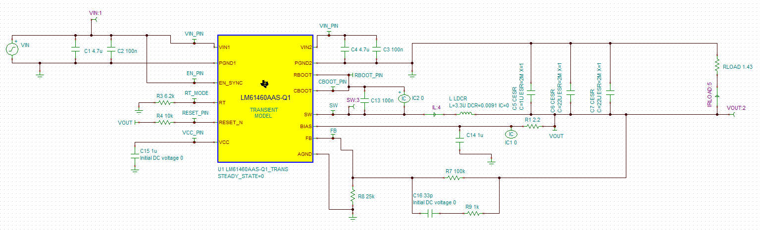
The TI LM61460-Q1 has an input range of 3V to 36V, up to 6A, variable output voltage, and controllable switching frequency.
Component selection largely followed the data sheets guidelines, with some initial value checks in TI’s Power Stage Designer. TI have also provided an excel calculator and TINA simulation models to help. I didn’t notice the excel calculator and sim files until near the end of layout so thankfully there weren’t too many changes. Only change was removal of the EN pin voltage divider to be directly connected to Vin. I don’t have a good guess on what transient load I’m expecting from the Pi so based it around a 2A value (1.5A up to 3.5A max). Transient load will be one to understand as the control system develops.
I ended up not using the enable voltage thresholds on the regulator. It’s marketed along the lines of allowing for a range of batteries and avoid deep discharge, for a 6S cell the enable and cut-off voltage levels didn’t really work with the hysteresis range of the IC and it also locked in the effective voltage range. There may have been some clever way to do it from the power distribution boards 3.3V output but I thought of it too late and may be trying to be too clever.
Though I ran some simulations with TI’s TINA software, the voltage input was not an accurate model of how the voltage will appear through the power distribution board. I will need to monitor how it behaves with real hardware for both comms board, PDB and with a battery. I will probably use an older Pi 3 as a sacrificial unit in case it goes sideways.
Initially I chose the switching frequency at 400kHz. This was for efficiency, the recommendation on component values, and it being under the AM band. After laying this out I realised it made more sense to go to a higher switching frequency which would allow me to get smaller components and the AM band isn’t relevant. I ended up with ~2MHz switching rate.
As there are leads of unknown length between the PDB adding an unknown inductance, I have added an electrolytic bulk capacitor at the input of the power connector.
CAN Buses
Each MCU are capable of interfacing with 3 FDCANs with a shared RAM module. However, 3 MCUs were used to distribute the communications load of devices from CAN and the other comms channels, 2 CAN channels each plus at least two SPI channels. I’ve not used the STM32G474s beyond the Nucleo boards so don’t have a firm grasp of how much load each can take with my programming capability. I wanted to have several CAN buses to distribute the CAN devices across, I’m not yet clear on what communication load is needed per each device so wanted to try and give myself plenty of headroom. This will depend on the required control loop update rate.
The SteadyWin motor drivers are capable of running CAN up to 1MHz with their software and CAN transceiver. The drivers STSPIN32G4 controller has unused FDCAN capabilities. The transceiver chosen for the comms board is the TI TCAN1057AV-Q1. This transceiver is capable of going above 5MHz, currently beyond my needs but wanted to use it as to allow flexibility moving forward as motors may change.
IMU
The IMU is crucial for the robot to have an understanding of how it (at least the torso) is actually oriented within the physical space.
I don’t think it needs to know where it is positioned beyond the local space so 6 axes is sufficient; with 3-axis accelerometer and 3-axis gyroscope and no magnetometer axes.
There are quite a few different options when it comes to IMUs. I ended up selecting the ST LSM6DSOX.
I was able to get a dev module with this that I can start to program and test with outside the comms board, using the Nucleo boards which should also help with any debugging too.
This IC has accelerometer range of ±2/±4/±8/±16 g full scale, and gyro range of ±125/±250/±500/±1000/±2000 dps full scale.
It also supports a range of communication protocols, I’ve implemented with SPI.
The device can also interface with external sensors or camera modules, with machine learning capabilities on board. These features all go beyond what I currently need, the equivalent without these extras were more expensive so it didn’t make sense to not choose this.
Once I’ve built up some familiarity with the core then I can always build on that in the future as needed with these features (if it still is in production).
MCUs
The MCUs chosen are the STM32G474RET6, the same used in the ST NUCLEO G474 boards. Both this version and the 48pin package had all the required peripherals exposed which could also have been used. Having the larger memory on board does give me more leeway for development without the risk of running out of space. While an optimisation challenge could be fun, I do need to remove some of the more unnecessary risks at this stage. Once I have something workable and a known code size to use as a benchmark, I could explore the value of using a smaller memory size (I expect the low volumes it’s likely negligible).
All the MCUs have their own debug connector for programming through STLink. The removal of the buttons I initially had for triggering reset means that I didn’t have an easy physical approach to reset. To help with this I put the NRST pin next to the GND pin in the connector, shorting these legs of the connector together will give the same effect.
External Connectors
To keep the board a bit more flexible in terms of functionality, along with knowing I want the robot to have a bit more in terms of lights and sounds in the future, I wanted to have some external connectors to enable this.
One is basically dedicated to connecting to a wireless module, with SPI, GPIO, and power. This could also be used for any other SPI or GPIO interface too.
Another for I2C, nothing in mind for what this could connect to, but a good opportunity to refresh myself with I2C as it’s been a long time since I last used it.
A final connector for 3.3V and 5V. Whether this is simply for powering something connected to one of the other connector or something that just needs some power.
Pi Interface
Nothing too crazy here, a large connector with the same pitch as the header pins on the Pi. My main concern is the current flowing between the pi and board and how the spacing of the ground pins will effect the overall signal integrity.
PCB
The board is being manufactured by JLCPCB. The fastest signals are the SPI buses and the CAN channels so should not need a a stack-up with super low dielectric materials or anything exceptional. I chose a 6 layer board as I wasn’t sure that I’d be able to fit all the routing in the space. The extra layers do add some cost to the board but the PCBs are cheap compared to the cost of components and the assembling.
The PCB layers were allocated as:
Top: Signal and power (very little portion)
Layer 2: Ground
Layer 3: Signal and Power (3.3V)
Layer 4: Ground
Layer 5: Signal and Power (5V)
Bottom: Ground
This stack up gave all signal layers bar the top layer a ground plane above and below. This helps with the signal integrity.
Simulation
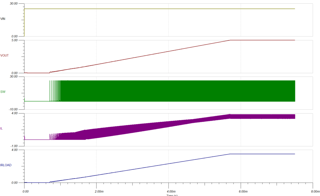
To build confidence in the values selected I ran simulations with the TI provided transient models in TINA. It took a while to get it set up and running as convergence issues would routinely pop up as components were changed. Changing components one by one with a record of changes was helpful to get to the schematic values, the order of removal seemed to be important to maintaining a runnable sim not just the components.
TI had two models, steady state transient with one input voltage, and a start up transient which had a ramp to the input voltage (over the span of nano and micro seconds). I ran a few simulations with different steady loads with the start up transient model. While it doesn’t take into account transient load swings of the Pi, or the true power source, it did build some confidence in the component values used.
The simulation did catch my misunderstanding in the thresholds of the Enable pin on the regulator. If the resistor values were kept as I had them, the package would never be enabled. I’m sure that would have been fun to debug on the hardware.
I also wanted to run some simulations for signal integrity to verify this behaviour. To get results that are trustable will require me to spend more time learning and playing around with programs such as Keysight’s ADS, none of which are cheap for licenses.
Stumbling blocks and learnings
Size was a big challenge. Trying to fit all the features and components into the space I wanted wasn’t achieved. I did look at a few areas to try and minimise the size but didn’t action on them.
These were:
- Smaller MCUs, I looked into using the STM32G474CET which has only 48pins in an LQFP form.
They were over double the price and had no stock at JLC.
Maybe one for a future revision. - Less CAN channels, looked at reducing from 6 to 5. It just didn’t seem enough of usable space saving to justify the loss of the channel. As I bring the board up with the rest of the system, it may prove that 6 channels is excessive/unused. This could be from either needs for the CNA bus channel or from the MCU requiring to allocate more resource to other peripherals leaving the 6th CAN bus only partially usable.
Sizing of output capacitance for the regulator was another area I struggled with.
The data sheet provides guidance on what size capacitance to use but in lieu of a known load transient I don’t have massive confidence that I have got what I need.
I always underestimate how long it takes to find and select the various different components. When derating comes in and poor data sheets, it can definitely be a trial of persistence.
Next Steps
Currently, the board is in production with JLCPCB, 4 blank PCBs and 6 PCBAs.
While they’re on their way there are a few things I want to get ahead of.
- Rough plan of build up for the Comms board and it’s software
- An initial start on firmware
- Some simulations of PDB providing the Comms board input
Other areas I want to try and investigate are:
- Reinforcement learning with the biped modified to have two feet and ankle actuators.
This is now runnable with Isaac Lab but with more refinement of the the program needed. - Review of the PDB design assumptions and values.
The system has become much more defined so should be able to have a more likely estimate than what I had, this can be coupled with the simulations.
I expect the head to have an additional controller installed to drive the head servos, lights, cameras or any additional peripherals that don’t make sense to run from the torso. If it is also built on top of a Raspberry Pi, my assumption and hope is that this communication could be done through ethernet. That would enable a clean physical implementation with only the need for this and power to travel between torso and head. It would also give me an opportunity to learn and apply the use of ethernet as the interface, something I have not done before.